 |
 |
 |
||||||
|
|
|
||||||
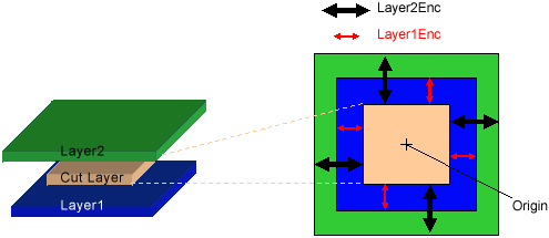
Standard vias are connections between two adjacent signal layers on the chip that are being connected. The cut layer is where the chip processing cuts away the oxide between the two adjacent signal layers to provide the connection between them. The layer enclosure via parameters specify the width and height for the rectangles on the conducting layers that lie above and beneath the cut.
For example, a Layer1 enclosure value of (10, 10) adds a spacing of 10 units around each side of the cut on Layer1. If the cut width and height are (1000, 2000), then the total size of Layer1 is (1020, 2020).
Use the corresponding get functions to return this information from the database.
Note: The layer number for the signal layers is not a via parameter. The layer number value is specified when the oaStdVia is created.
This example shows the origin at the default location with a (0,0) offset.
If using an origin offset, that offset is added to every part of the via,
and the relative locations are unchanged. For vias that require Layer1 or
Layer2 rectangles that are not centered at the cut center, use the
Layer1 Offset or
Layer2 Offset parameters.
Return to Programmers Guide topics

Copyright © 2001-2010 Cadence Design Systems, Inc.
All rights reserved.